
Contents
When I first stumbled upon Graph Theory, it was through a tangled mess of electrical wires on my workbench. I had no idea that those chaotic lines had anything to do with math. But then I discovered that every circuit I was building was secretly a graph—nodes connected by edges. That’s when everything clicked.
In simple terms, Graph Theory is the study of graphs—structures made up of vertices (or nodes) and edges (the connections between them). Think of it like a map of relationships. Whether you’re looking at social networks or power lines, you’re probably dealing with a graph.
Now, here’s the cool part for us in electronics: circuits can be modeled as graphs. This helps in analyzing the layout, optimizing the connections, and even detecting faults. For example, using Planar Graphs, we can visualize circuits without overlapping wires—a dream for PCB designers. But not all circuits are that neat, and that’s where Non-Planar Graphs come into play.
In this article, I’ll walk you through the basics of Graph Theory, how Electrical Circuits can be represented as graphs, and the difference between Planar and Non-Planar Graphs. We’ll also touch on practical applications that make all this theory worth knowing.
What is a Planar Graph?
Imagine trying to draw a map of a subway system where no two lines overlap—sounds impossible, right? Well, that’s exactly what a Planar Graph aims to do. In the world of Graph Theory, a Planar Graph is one that can be drawn on a flat surface without any of its edges crossing, except at the vertices where they meet.
Formally speaking, a Planar Graph is a graph that admits a planar embedding. That means there exists a way to position its vertices and draw its edges in the plane such that no two edges intersect except at their endpoints. This might sound abstract, but it has very real implications—especially in designing Electrical Circuits or creating road networks that are easy to navigate and construct.
To give you a visual example, think of a triangle with a dot in the middle connected to all three corners. That’s a Planar Graph. But try doing that with five dots where each one connects to every other—no matter how hard you try, you’ll end up with overlapping lines. That’s when things move into the realm of Non-Planar Graphs.
The ability to create a layout with minimal edge crossings isn’t just mathematically elegant—it’s also a big deal in real-world applications. Whether you’re designing circuit boards or laying out a metro map, Planar Graphs help you make systems clean, efficient, and visually understandable.
Illustrative Examples of Planar Graphs
One of the first times I truly appreciated Planar Graphs was while sketching out a simple electrical circuit during a college project. I had a battery, three resistors, and a couple of wires. When I connected the components, I realized the entire setup could be drawn in a way where none of the wires overlapped. That was my first encounter with a real-world planar graph without even knowing the term for it.
Here’s the example: Picture a triangle where each corner represents a resistor and each side a wire. Connect a battery to one of the corners—voilà! You’ve got a Planar Graph. All components are connected, and yet, no edges (or wires) intersect unless they’re supposed to. Clean, simple, and functional.
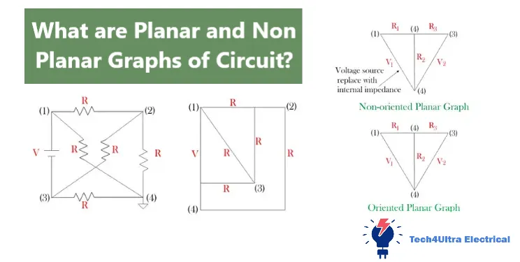
Now let’s take it up a notch with mesh analysis, a method used in circuit theory to calculate current in loop-based systems. It works beautifully with Planar Graphs because each mesh (closed loop) can be easily traced without ambiguity. With non-overlapping loops, identifying independent meshes becomes a breeze. This makes the math easier, reduces the chance of mistakes, and helps in clearly labeling voltage drops and current directions.
If you’re working with circuits or even just love clean visual layouts, understanding how to recognize and use Planar Graphs can seriously elevate your design game—whether it’s physical or purely theoretical.
What is a Non-Planar Graph?
If you’ve ever tried drawing a circuit layout and found yourself looping wires awkwardly over one another, chances are you were working with a Non-Planar Graph. By definition, a Non-Planar Graph is one that cannot be drawn on a flat surface without some of its edges crossing—no matter how creatively you try to arrange the vertices.
The key condition that defines a Non-Planar Graph is that it lacks a planar embedding. This means it’s impossible to connect all its vertices with edges that only meet at their endpoints without overlaps. These edge crossings aren’t just aesthetic problems—they can cause real issues in electrical circuits, especially in densely packed PCBs where clarity and space are critical.
Enter Kuratowski’s Theorem, the formal backbone of this concept. The theorem states that a graph is non-planar if it contains a subgraph that is a subdivision of either K5 (a complete graph with five vertices) or K3,3 (a complete bipartite graph). These two are the ultimate red flags in graph theory—if you find either hiding in your design, you’re not going to avoid edge crossings.
Understanding Non-Planar Graphs isn’t just for mathematicians. For engineers and designers, it’s a reality check. If your circuit looks like spaghetti, it’s probably time to reconfigure—or accept that you’re dealing with a layout that just refuses to behave.
Understanding Kuratowski’s Theorem and Its Applications
Let’s be honest—graph theory can get a little abstract. But Kuratowski’s Theorem? It’s surprisingly practical once you know what to look for. This theorem tells us exactly when a graph crosses over from neat and tidy (planar) to messy and unmanageable (non-planar).
The heart of it lies in two specific “forbidden” graphs: K5 and K3,3. The first, K5, is a complete graph with five vertices where every node connects to every other node. Imagine trying to connect five people where each one shakes hands with all the others—without any arm crossings. Not happening. That’s non-planar.
The second, K3,3, is a complete bipartite graph. It’s like dividing six nodes into two groups of three and drawing lines between every node in one group to every node in the other. Still impossible to draw cleanly without overlaps. Spot either of these configurations—or their “subdivisions”—in your graph, and you’ve officially crossed into non-planar graph territory.
So how do you apply Kuratowski’s Theorem in real situations like electrical circuits?
- Step 1: Simplify your graph. Remove unnecessary nodes and edges that don’t affect the core structure.
- Step 2: Look for subgraphs resembling K5 or K3,3. Even if they’re distorted or have extra vertices along the edges, they count.
- Step 3: If one exists, your graph is non-planar. Time to reconsider your layout or prepare for edge crossings.
Kuratowski’s Theorem might sound intimidating at first, but once you start recognizing these graph shapes in your designs, you’ll see why it’s one of the most powerful tools in the graph theory toolbox.
Examples of Non-Planar Circuits and How to Recognize Them
I remember the first time I built a Wheatstone bridge and tried to sketch it on paper—it looked like a bowl of spaghetti. That’s when I learned I was dealing with a non-planar graph. Circuits like the Wheatstone bridge, full adders, and certain amplifier networks often fall into this category due to how components interconnect in overlapping loops.
What makes these electrical circuits non-planar is the number of interdependent paths. When more than four or five components connect in multiple closed loops, the chance of needing edges to cross increases. Unlike planar graphs, there’s simply no way to rearrange the components so that connections don’t overlap somewhere.
The edge crossing issue isn’t just a visual headache—it can also lead to physical layout problems on PCBs, like unwanted interference, noise, and signal integrity issues. That’s why identifying the graph type early is critical in circuit design.
Thankfully, we’ve got tools to help. Software like KiCad, LTspice, and Multisim can simulate and visually map out your circuit, revealing overlapping connections that hint at non-planar graphs. For more mathematical accuracy, tools like Graphviz or NetworkX in Python can analyze your graph structure and help you spot K5 or K3,3 configurations.
If your circuit sketch looks like a mess of wires no matter what you do, chances are you’re staring at a classic non-planar graph. Embrace the chaos—just use the right tools to manage it.
Read Also: Understanding Space Charge: Effects, Laws, and Applications in Modern Electronics
Comparison: Planar vs Non-Planar Circuits
When designing electrical circuits, understanding whether you’re dealing with a planar graph or a non-planar graph can seriously impact your layout and analysis. Here’s a quick side-by-side breakdown:
- Planar Circuits: Can be drawn without edge crossings. Ideal for clean PCB designs and easy visual tracing.
- Non-Planar Circuits: Require overlapping edges when drawn. Common in complex logic or multi-stage amplifier systems.
- Planar Graphs: Easier to apply mesh analysis and solve loop equations.
- Non-Planar Graphs: May need advanced solving techniques like nodal analysis due to tangled loops.
- Planar Design: Reduces risk of signal interference and crosstalk in high-frequency circuits.
- Non-Planar Design: Demands more layers in PCB layout or creative rerouting to avoid shorts.
In short, planar circuits are your friend when simplicity matters. But don’t panic when things get non-planar—just know you’ll need a bit more planning and maybe a layer or two more on your PCB stack-up.
Why It Matters in Electrical Engineering
At first glance, graph theory might seem like a purely academic topic—but in electrical engineering, it plays a much bigger role than most people realize. Especially when it comes to PCB design, knowing whether you’re working with a planar graph or a non-planar graph can make or break your circuit layout.
When dealing with planar circuits, you can route traces on a single layer without overlaps. That means fewer vias, less interference, and lower production costs. On the other hand, non-planar circuits often require multi-layer boards and careful routing to avoid shorts and ensure signal integrity. This not only increases complexity but also impacts thermal management and manufacturing time.
Beyond layout, graph classification also influences how we analyze circuits. For instance, mesh analysis becomes more intuitive and efficient in planar graphs because each independent loop can be traced cleanly. Try that with a non-planar graph, and you might find yourself rechecking your loops ten times to avoid errors. That’s where nodal analysis often steps in, especially when planar simplification isn’t an option.
In short, understanding graph types isn’t just a theoretical exercise—it directly affects how you build and test your designs. If you care about cleaner PCBs, faster analysis, and fewer headaches, then trust me: graph theory is your secret weapon.
How to Transform a Non-Planar Graph to Planar (If Possible)
So you’ve got a non-planar graph messing up your circuit design. Can you fix it? Sometimes—yes. The trick lies in clever redrawing and strategic use of dummy nodes. These techniques can occasionally help you turn chaos into a clean planar graph.
One approach is to add dummy nodes at edge intersections. Instead of letting two wires cross, you introduce a new vertex where they meet, effectively breaking the edge into two. This technique can simplify the graph just enough to allow a planar embedding.
Another method is redrawing the graph using tools like Graphviz or yEd, which attempt to find non-overlapping layouts automatically. These are especially helpful for reconfiguring electrical circuits into more manageable PCB layouts.
But here’s the catch: not all non-planar graphs can be fixed this way. If the structure includes a true K5 or K3,3 subgraph, no amount of trickery will make it planar. At that point, you’re better off accepting the complexity and planning a multi-layer board.
In the end, transforming a graph is more about managing complexity than eliminating it. Sometimes, a little creative layout can go a long way—but know when to let go and design smart instead.
Conclusion and Takeaways
By now, it’s clear that knowing the difference between a planar graph and a non-planar graph isn’t just theoretical—it’s a practical skill in electrical circuit design and analysis. Planar circuits simplify PCB layouts and make techniques like mesh analysis more effective, while non-planar circuits demand advanced planning and often rely on nodal analysis.
Understanding the structure of your graph—whether it includes a hidden K5 or K3,3—can save you from headaches in both design and troubleshooting. It also helps you make smarter choices in tool selection and simulation workflows.
In the end, graph theory isn’t just math on paper. It’s a lens through which we see, build, and refine the systems that power our world. The better you understand it, the better engineer you’ll become.
Common Misconceptions and FAQs
Is every circuit graph planar?
Absolutely not. It’s easy to assume that every electrical circuit can be drawn without overlaps, especially when working with simple diagrams. But as complexity grows—more components, more connections—you’ll run into non-planar graphs. Think of bridge circuits or full-adder designs; they often include configurations like K5 or K3,3 that make planarity impossible.
Can a non-planar circuit be analyzed with the same techniques?
Yes, but with caveats. While mesh analysis thrives in planar graphs, it becomes messy with non-planar circuits due to overlapping loops. That’s where nodal analysis shines—it focuses on voltages at nodes, making it ideal when planar simplification isn’t possible. The technique doesn’t care about planarity; it just needs consistent node labeling and current directions.
Does planarity affect simulation software outputs?
Surprisingly, not really. Tools like LTspice or Multisim are focused on logic and math, not visual structure. Whether your circuit is planar or not, as long as connections are valid, the simulation will run. However, planarity does affect your experience. Cleaner layouts mean easier debugging, quicker edits, and a better understanding of current paths during simulation.
So while planarity doesn’t change the math behind your circuit, it definitely changes how you interact with it. It’s not a requirement—but it’s a huge bonus when things are neat, visual, and manageable.
What is the difference between planar and non-planar circuits?
Planar circuits can be drawn on a flat surface without any wires crossing over each other, making them simpler to design and troubleshoot. In contrast, non-planar circuits involve connections that inevitably overlap, often requiring multi-layer PCBs or creative routing solutions to maintain clarity and functionality.
What is planar and non-planar graph in network analysis?
In network analysis, a planar graph allows for easier loop identification and is ideal for applying mesh analysis. A non-planar graph, however, includes complex interconnections that lead to overlapping paths, making mesh analysis harder and often requiring nodal analysis instead. Recognizing these structures helps engineers choose the right analytical approach.
What is planar and non-planar?
Simply put, planar refers to any graph or structure that can be represented without edge crossings on a 2D plane. Non-planar means that such a representation is not possible without overlaps. In electrical circuits, this distinction affects how cleanly a system can be visualized, built, and analyzed.
Can mesh analysis be used for planar or nonplanar?
Mesh analysis is best suited for planar circuits, where loops are easily defined without overlapping wires. While technically possible in non-planar circuits, it’s often impractical due to tangled meshes and ambiguous paths. In those cases, nodal analysis becomes the preferred method for accuracy and simplicity.