Contents
You know that moment when you plug in a device, and it just works—no sparks, no glitches, just smooth electrical magic? Behind that seamless performance lies a concept that might sound a bit intimidating at first: space charge.
Space charge refers to the accumulation of electric charge in a region, usually between electrodes, due to limited mobility of electrons or ions. It’s a big deal in vacuum tubes, capacitors, semiconductors—basically anything that deals with current flow. In simple terms, it’s like traffic congestion, but instead of cars, it’s electrons getting jammed up in a region they’re not moving through fast enough.
This phenomenon is particularly critical in systems where thermionic emission occurs—like in a vacuum diode, where heated cathodes release electrons that pile up and create this charge cloud. This leads us to Child’s law, which explains how current in a vacuum is related to the voltage and distance between electrodes, assuming the current is limited by the space charge itself.
When we shift from vacuum systems to solids or dielectrics, the principles extend. The Mott–Gurney law describes similar behavior in solid-state devices, specifically regarding space-charge-limited current in insulators or semiconductors. If not managed properly, the buildup can even result in dielectric breakdown, damaging the system entirely.
In this blog, I’ll break down these concepts through real-world examples and a bit of personal trial and error (because yes, I’ve fried a component or two). Whether you’re an engineering student or just curious about what happens inside your gadgets, you’re in the right place.
Read also: Star Delta Starter: Comprehensive Guide to Working, Circuits, and Applications
What is Space Charge?
When I first stumbled across the term space charge, I was deep into a late-night rabbit hole on vacuum tubes and electron beams. Honestly, it sounded more like something out of a sci-fi movie than a physics topic. But understanding it changed how I saw thermionic emission and electronic devices entirely.
So what is space charge really?
The Reality Behind Space Charge
Imagine you’re heating up a metal filament in a vacuum tube (yeah, like those old-timey radios or CRT monitors). As it heats, electrons start jumping off the surface. This process is called thermionic emission, and it’s like the electrons are escaping from jail because of the heat energy.
Now here’s the kicker: those freed electrons don’t just zip away neatly. Nope—they build up in the region near the surface, creating a negatively charged cloud. That’s your space charge. It’s basically a crowd of electrons that repel other electrons trying to follow. So instead of helping, they actually block more electrons from escaping.
And that’s not just a fun fact—it totally messes with how much current you can get through the device.
“Electrons behave like people at a concert. Too many in one area, and nobody else can get in.”
How Child’s Law Explains It
This is where Child’s Law steps in and saves the day—sort of. I remember miscalculating current flow in a diode project because I ignored space charge effects. Turns out, Child’s law (also called the Child–Langmuir law) gives you a formula to predict the maximum current that can flow when space charge is a factor.
J = (4ε₀/9) * sqrt(2e/m) * (V^3/2 / d²)
Where:
– J is the current density,
– V is the applied voltage,
– d is the distance between the electrodes.
This equation showed me how voltage and distance between plates control current, especially in vacuum devices. If you crank up the voltage or bring plates closer, more current gets through, but there’s always that space charge limit.
Takeaways From My Mess-Ups
I made some classic mistakes:
- Ignored space charge in my thermionic diode design. Current didn’t rise as expected.
- Forgot Child’s law exists. Cost me a week of troubleshooting a lab circuit.
- Assumed thermionic emission alone determines current—it doesn’t.
So here’s what I’d tell my past self:
- Always consider space charge in low-pressure or vacuum systems.
- Use Child’s law when estimating current limits—it’s not just academic.
- Recognize that thermionic emission is only step one in a multi-step drama.
In short, space charge isn’t just theoretical fluff. It’s a real effect that shapes how devices work. Whether you’re designing old-school tubes or futuristic electron guns, ignoring it is like building a dam and forgetting about the water pressure behind it.
Physical Origin of Space Charge
To understand how space charge forms, we need to zoom in to the atomic and subatomic level. At the heart of it, it all starts with the movement—or lack thereof—of charged particles like free electrons and ions. When an electric field is applied across a material, electrons start to move. But if they can’t move freely, they begin to pile up in certain regions. This imbalance creates what we call space charge.
Free electrons play a central role here. In conductive or semi-conductive materials, they respond quickly to electric fields. But in vacuum tubes or insulators, their movement is restricted. As these electrons accumulate, they form a negative space charge. This collection of excess electrons actually starts to repel new electrons, limiting the current that can flow—a behavior that’s described well by Child’s law and the Mott–Gurney law.
On the flip side, when we talk about the absence of electrons or the presence of positive ions in a region, we encounter a positive space charge. Both types—positive and negative—affect how voltage and current behave in a system.
The formation of space charge isn’t just limited to solids or semiconductors. It’s a big factor in vacuum devices like the vacuum diode, where thermionic emission causes hot electrons to fly off a heated surface, only to gather and slow each other down. If this buildup becomes intense enough, it can even lead to dielectric breakdown in surrounding materials.
So yeah, the next time you see current lagging or strange voltage drops, think microscopic—space-charge-limited current might just be at play.
Mechanisms of Space Charge Generation
Let’s get into the gritty details—how does space charge actually come into being? One of the main culprits is thermionic emission. This happens when a material (usually a metal) is heated to the point that its electrons gain enough energy to escape from the surface. Think of it like popcorn kernels bursting when heated—those hot, energetic electrons jump out and form a cloud near the emitting surface, especially in devices like the vacuum diode.
Another major source is charge injection from electrodes. When a high enough voltage is applied across an insulating material or semiconductor, electrons or holes are “injected” from one electrode into the bulk of the material. These carriers move under the electric field, and if they can’t exit fast enough, they start to accumulate—voilà, more space charge.
Temperature plays a huge role here. As temperature increases, more carriers are excited thermally, boosting thermionic emission and enhancing mobility. But material properties matter too—some materials trap charges or have low mobility, making them more prone to space-charge-limited current. That’s why different materials behave so differently under the same conditions, especially in high-voltage or thin-film applications governed by the Mott–Gurney law.
It doesn’t end there. Other factors like radiation can knock electrons loose, adding to the charge pool. Polarization effects in dielectrics can also disturb the local electric field, shifting how charges move or accumulate. And when things get out of hand, it might all spiral into dielectric breakdown.
So yeah, whether it’s heat, voltage, or the quirks of your material, the creation of space charge is usually a mix of these intertwined effects. It’s like a recipe where changing one ingredient messes with the whole dish—just at the scale of atoms and electrons.
Space Charge Regions and Their Properties
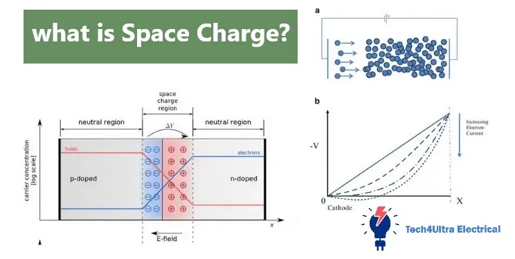
Alright, let’s talk geography—but on a microscopic scale. In semiconductors and insulating materials, space charge often forms distinct regions: the depletion region and the accumulation region. These aren’t just labels—they behave very differently and have huge effects on how devices work.
The depletion region is where mobile charge carriers (like electrons or holes) have been pushed out. It’s kind of like a ghost town—low in free charges but packed with immobile ions, which creates a strong internal electric field. On the flip side, the accumulation region is where charges gather, like a crowded subway. This dense charge cloud shifts the local electric potential and messes with current flow.
The electric field across these regions isn’t uniform. It typically increases across the depletion region, reaches a peak, then drops off. This gradient affects how other charges move and is central to device behavior in things like diodes and transistors.
Then comes the concept of band bending. When space charge forms, the energy bands of the material bend to reflect the change in electric potential. That’s why you see band diagrams showing those familiar curved lines—especially in p-n junctions or near metal contacts. This band bending explains the potential distribution and helps predict carrier motion under external bias.
In short, space charge regions aren’t just theoretical—they’re the invisible scaffolding that defines how electronic devices behave. Understanding these regions is key to unlocking the behavior of everything from vacuum diodes to modern semiconductors.
Space-Charge-Limited Current (SCLC)
In Vacuum Systems (Child–Langmuir Law)
Let’s start with the classics—vacuum tubes. In these systems, space-charge-limited current is beautifully described by the Child–Langmuir law (often just called Child’s law). The basic idea? When electrons are emitted from a hot cathode via thermionic emission, they don’t move freely forever. As they travel toward the anode, their own negative charge creates a repelling electric field that slows new electrons down. This limits the total current that can flow.
The Child–Langmuir law gives us a clear formula: the current density J is proportional to the voltage V raised to the 3/2 power, divided by the square of the distance d between electrodes. That’s J ∝ V3/2 / d2. But here’s the catch: this assumes a perfect vacuum, no initial electron velocity, and one-dimensional flow.
This model laid the foundation for vacuum tube design and early electronics. Every vacuum diode follows these principles—if you ever mess with old radios or cathode-ray tubes, you’re seeing Child’s law in action.
In Semiconductors and Insulators (Mott–Gurney Law)
Things get more complicated in solids. When current flows through an insulator or semiconductor, space charge also builds up—but the rules are different. Enter the Mott–Gurney law. It describes space-charge-limited current in a trap-free insulator where charge carriers are injected from an electrode and drift through the material under an applied field.
The current density here also follows a voltage-squared relationship: J ∝ V2 / d3. But real-world materials often have traps—defects or impurities that “catch” free carriers. That’s where things shift. In trap-filled conditions, the current increases more slowly until the traps are saturated. Only after that do we see behavior consistent with the Mott–Gurney model.
Devices like organic LEDs and thin-film transistors rely on this understanding. By engineering materials with fewer traps—or controlling injection—we can optimize current flow and efficiency.
Still, the Mott–Gurney law has its limits. It assumes uniform carrier mobility and no recombination, which isn’t always the case. But even with its imperfections, it’s a powerful tool for modeling how space charge shapes current in modern electronics.
Space Charge in Practical Applications
Let’s step out of theory and into the real world—because space charge isn’t just textbook jargon. It plays a critical role in some of the tech we rely on daily, especially in high-voltage and energy-efficient devices.
First off, in high voltage insulation, space charge can be a real headache. When electric fields stress an insulating material, charges can get injected from the electrodes and become trapped. These charges distort the internal electric field, sometimes leading to dielectric breakdown. Engineers use this knowledge to design better insulators for power lines, transformers, and high-voltage cables that last longer and fail less often.
Next up: capacitors and dielectric materials. In high-performance capacitors, managing space charge means better energy storage and reduced leakage. Materials are carefully chosen or engineered to resist unwanted charge accumulation that could cause losses or breakdowns.
Then we’ve got organic semiconductors—a big deal in flexible electronics and displays. These materials often suffer from traps and variable mobility, which makes space-charge-limited current a major factor in their design. Using models like the Mott–Gurney law, researchers can optimize layer thickness, electrode materials, and even the choice of organic compounds.
Finally, think of solar cells and OLEDs. In both cases, charge injection and accumulation affect how efficiently electrons and holes reach the active region. Poor control over space charge can mean lower brightness, shorter lifespans, or reduced energy conversion. That’s why advanced devices include buffer layers or charge-blocking layers to keep the flow just right.
Bottom line: space charge isn’t just a problem to solve—it’s a design parameter. Mastering it means unlocking better performance across a wide range of electronic and energy systems.
Measurement and Analysis Techniques
So how do we actually see space charge—something that’s invisible and microscopic? That’s where specialized techniques come in. Detecting and quantifying space charge isn’t easy, but it’s essential for understanding material behavior under electric fields.
One of the most commonly used methods is Thermally Stimulated Depolarization Current (TSDC). This technique involves cooling a dielectric material while applying a field, then slowly heating it up. As trapped charges are released, they generate a measurable current. Peaks in the current vs. temperature curve give insights into trap depth and charge distribution.
Another powerful tool is the Pulsed Electroacoustic (PEA) method. A high-voltage pulse generates an acoustic wave through the material, which carries information about internal charge distribution. By detecting this signal with a sensitive transducer, researchers can map the space charge profile across the sample.
Other methods include the Laser-Induced Pressure Pulse (LIPP) technique and Electro-Optic methods, depending on material transparency and sensitivity needs. Each has its own pros and cons, but together they offer a full picture of how space charge forms and evolves over time.
These tools are critical in industries like power insulation, electronics, and materials science, helping engineers refine designs and prevent failures.
Effects and Implications of Space Charge
When it comes to electronics, space charge can be both a symptom and a cause of deeper issues. One of its biggest impacts is on device performance. Whether you’re dealing with vacuum diodes or solid-state devices, accumulated charge distorts internal electric fields, alters carrier flow, and shifts voltage thresholds. In short: it messes with the predictability and efficiency of your device.
In high-voltage systems, space charge contributes directly to dielectric breakdown. As injected charges accumulate and distort the field, they can create localized hotspots where the electric field exceeds the material’s limit. One small crack, and you’ve got a catastrophic failure. This is especially critical in insulation materials used in power grids and aerospace components, where breakdowns aren’t just inconvenient—they’re dangerous.
And then there’s long-term reliability. Space charge can lead to aging effects in capacitors and semiconductors, reducing their lifespan. Charge traps can cause hysteresis, drift in characteristics, and even performance degradation over time. In devices using organic materials—like OLEDs and solar cells—this can mean dimmer screens, lower efficiency, or sudden malfunctions.
Engineers often design around space-charge-limited current effects, using buffer layers, optimized geometries, or material blends to reduce buildup. But ignoring it? That’s never a good idea. It’s like letting dust build up in your computer—it may not crash today, but it’ll get you eventually.
Mitigation and Control Methods
Managing space charge isn’t about eliminating it completely—because you often can’t. It’s about controlling where and how it forms. One key strategy is material engineering. By selecting materials with low trap densities or high mobility, you reduce unwanted charge buildup. For example, using polymers with tailored dielectric properties or doping semiconductors can dramatically improve charge transport.
Geometrical optimization also plays a big role. In vacuum diode design or layered devices like OLEDs, adjusting the thickness of insulating layers or the spacing between electrodes can minimize the effect of space-charge-limited current. Tapered structures or gradient doping profiles can help redistribute electric fields more evenly.
Then there’s tuning your operational parameters. Reducing voltage, managing pulse durations, or controlling temperature can limit thermionic emission or slow charge injection. For high-voltage applications, engineers often limit ramp rates or apply conditioning protocols to “pre-form” stable charge distributions.
Combining these approaches—smart materials, good design, and careful operation—can keep space charge in check and extend the life and reliability of critical electronic systems.
Future Trends and Research Areas
The role of space charge is only growing as devices shrink. In nanoscale electronics, even a small amount of trapped charge can dominate the behavior of the entire system. Researchers are now focused on understanding space-charge-limited current in ultra-thin films, nanowires, and 2D materials where traditional models like Child’s law and the Mott–Gurney law start to break down.
Emerging materials like perovskites, organic blends, and advanced polymers are pushing the boundaries of what’s possible—but they also come with new challenges in charge transport and stability. As a result, better modeling techniques are being developed that account for trap dynamics, field-dependent mobility, and quantum-scale effects.
Whether in flexible displays or energy-harvesting devices, managing space charge at the nano level is set to define the next generation of electronics.
Watch also: System of Wiring: Types, Uses, and Tips
Conclusion
From thermionic emission in vacuum diodes to current flow in organic semiconductors, space charge plays a central role in modern electronics. We’ve explored how it forms, how it limits current via Child’s law and the Mott–Gurney law, and how it impacts device performance, reliability, and safety through phenomena like dielectric breakdown.
Whether you’re working on high-voltage insulation or cutting-edge nanoscale devices, understanding space-charge-limited current is key. It’s not just a theoretical concept—it’s a practical design constraint and a tool for innovation.
Engineers must continue to find smarter ways to manage space charge through material science, geometry, and operational strategy. The challenge is real, but so is the opportunity to improve everything from power systems to flexible electronics.
FAQs
What do you mean by space charge?
Space charge refers to the accumulation of excess electric charge in a region, typically between electrodes, due to limited movement of electrons or ions. This buildup creates internal electric fields that can influence current flow and device behavior.
What is the space charge effect?
The space charge effect occurs when accumulated charge alters the local electric field, limiting the flow of additional charge carriers. In vacuum tubes or semiconductors, this often leads to space-charge-limited current, where the current is no longer controlled by voltage alone but also by the repulsion between like charges.
What is space charge in photoelectric effect?
In the photoelectric effect, space charge can form when photoemitted electrons build up near the emitting surface, especially at high intensities. This cloud of negative charge repels further emission and can reduce the effective current, altering the system’s efficiency.
What is the space charge area?
The space charge area is a specific region within a material or device where this charge buildup occurs. It could be a depletion region in a semiconductor, the gap in a vacuum diode, or a localized zone in a dielectric exposed to high fields. The properties of this area heavily influence how voltage and current behave across the device.
2 thoughts on “Energy Quanta: The Foundation of Quantum Theory”